VIA NEXT
Manufacturing Design
We provide:
Production Management
Package Design
Failure Analysis
Reliability Testing
Design for Manufacturing
Production Management
VIA NEXT can assist in managing the complexity of manufacturing advanced semiconductor products.
From facilitating information exchange with wafer manufacturing, packaging and testing partners, to streamlining technology, schedule, quality, and materials management, VIA NEXT is your partner throughout the entire manufacturing process.
We provide:
- PPA-Based Foundry and Process Evaluation and Selection
- Chip Architecture and Circuit Evaluation And Review
- Target Yield, Reliability, Cost Structure Proposal and Evaluation
- WAT and Corner Lot Review
- Manufacture Process and Cost Optimization
Design for Manufacturing
Package Design
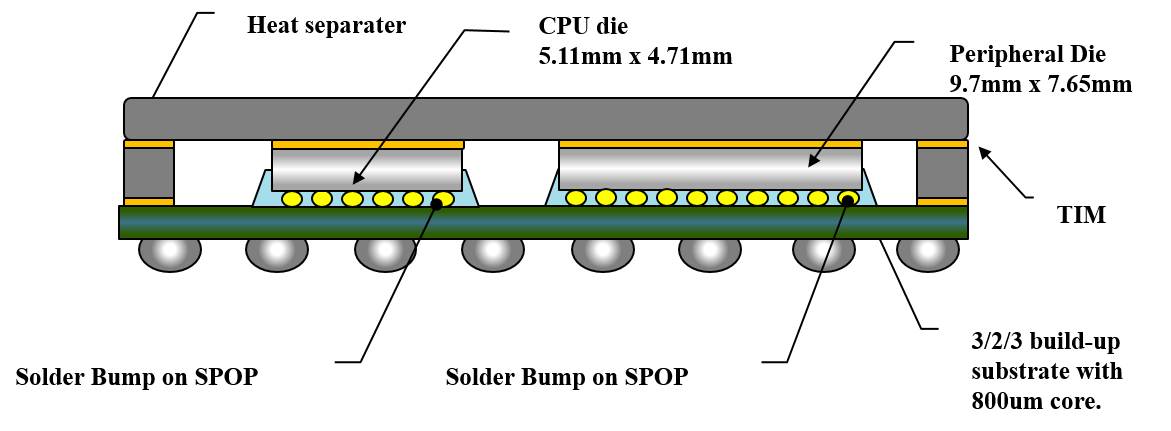
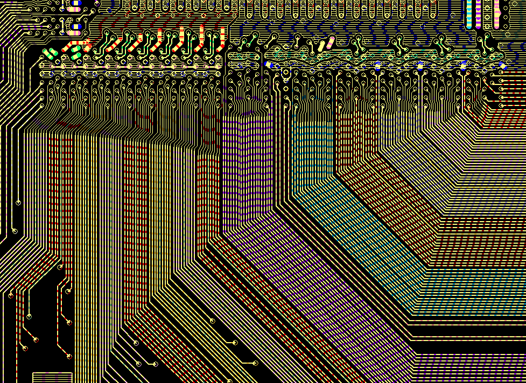
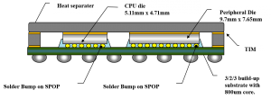
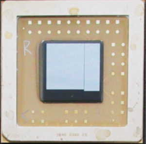
As the requirements of modern IC design become more demanding, VIA NEXT’s expertise in the design and development of complex chip packages means that we can assist in developing the most suitable package design for your product applications.
We provide:
- Package and Substrate Design
- Single-Chip, Multi-Chip (Let), Hybrid-Type, Wafer-Level and Heterogeneous Integration Packages
- Package on Package (POP) and System in Package (SIP) Integration
- Chip-Package-System Co-Development
- Chip and System Thermal Solution
Design for Manufacturing
Failure Analysis
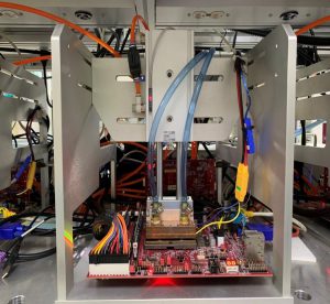
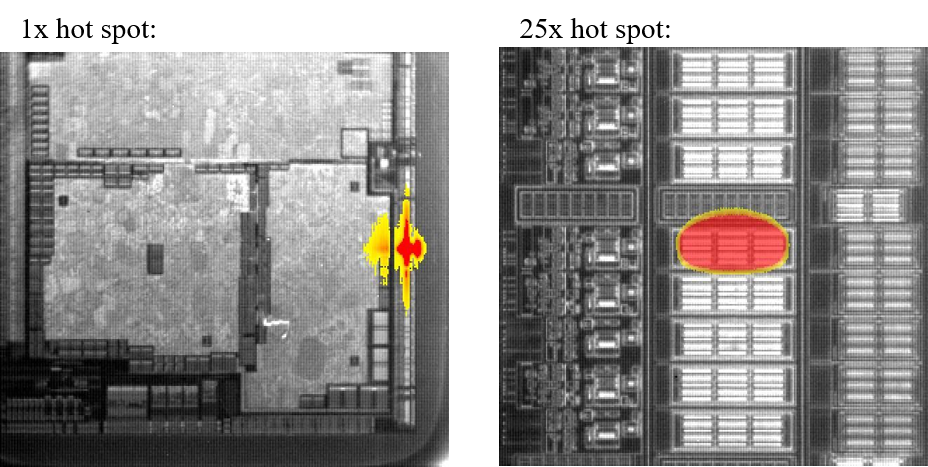
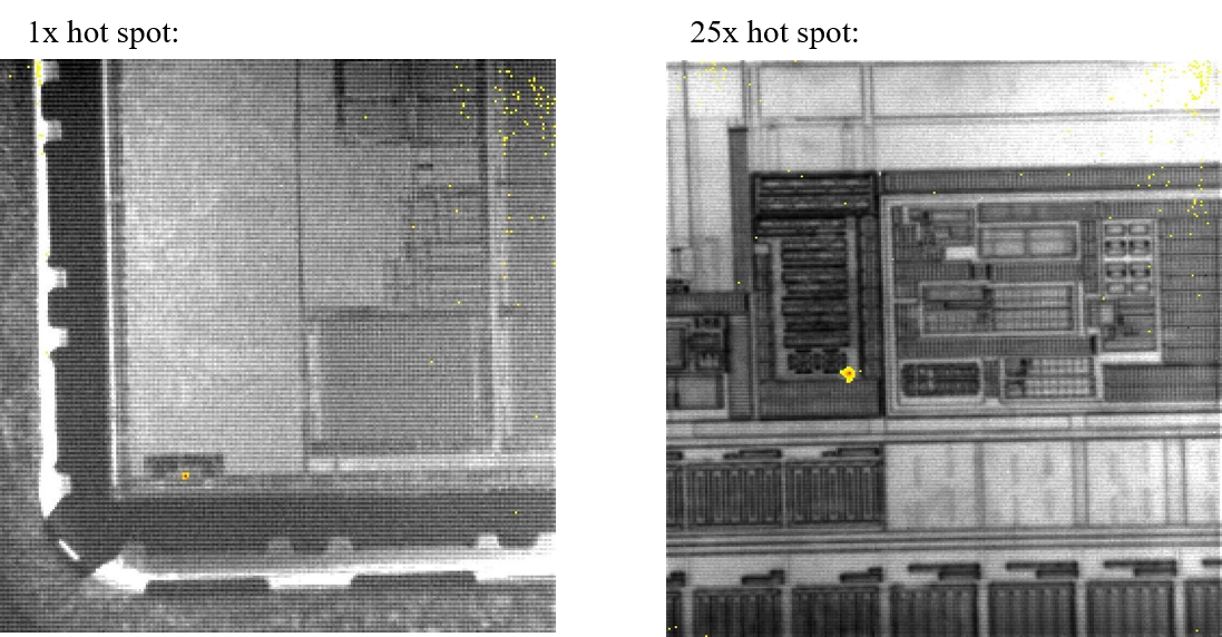
VIA NEXT provides comprehensive, industry-leading failure analysis services to ensure that you can make your products more robust when things go wrong.
We provide:
- Industry Partnerships and Expertise in Failure Analysis and Debugging
- One-Stop Failure Analysis Services
- Chip Circuit, Substrate, Package, and System Failure Analysis
Design for Manufacturing
Reliability Testing
By partnering with VIA NEXT, we can ensure that your IC design meets stringent production requirements and is robust throughout the entire product lifecycle.
We provide:
- ESD/Latch-up/HTOL/EFR Testing Platform Design
- ESD/Latch-Up Circuit Preview
- HTOL/EFR Operation and Test Report
- ESD HBM/MM/CDM and Latch-Up Test Plan
- Post-Test Failure Analyses for ESD/Latch-Up/Reliability Tests
